Career
Application Guidelines
Non
Non
| Positions | Information system |
| Number of positions | 1 |
| Job Description | Works related to company's information systems (installation, construction, operation and maintenance) as follows: ・Construction, management and operation of internal IT infrastructure (e.g. servers and networks); ・Installation, operation, and maintenance of internal information systems; ・Management and procurement of software licenses for internal use; ・Management and procurement of IT devices (PCs, monitors, etc.) and supplies; and ・Operations of helpdesk for our employees Operation of information security: ・Operation of internal information security in general (operation of ISMS); ・Monitoring by asset management tools |
| Requirements | ・Work experience at an organization handling information systems for its internal use: Experience in planning, designing, constructing, and operating IT systems, as well as upstream design and overall management of IT system administration. ・IT infrastructure engineering skills (for server, network and PCs): Work experience in handling Windows PC, Windows, and Linux server environment Work experience in handling network such as FW, switch, wireless LAN environment, etc. ■Preferred qualifications ・Review of various systemization for business improvement ・Information literacy education ・Development of internal systems ・Work experience in installation and operation of financial accounting systems |
| Employment Type | Full-time |
| Educational background | High school graduate or above |
| Location | Kyushu Operation Center (Ashikita-machi, Ashikita-gun, Kumamoto) |
| Working hours | 8:30 - 17:15 (with flextime system) |
| Salary and allowance | Monthly base salary: 250,000 yen to 370,000 yen (determined by our rules based on your experience and other factors) Various allowances: Overtime allowance, Role pay, Family allowance, Commuting allowance, and Meal allowance (in accordance with our rules) |
| Benefits | Various insurance (health, welfare, employment, and workers' compensation) Savings support program, Defined contribution pension plan, Retirement allowance, Cafeteria plan, Language Learning support |
| Salary increase | Once a year |
| Bonus | Twice a year (June and December) |
| Leave/Vacation | 2 days off per week (Saturdays & Sundays), National holidays, Special holidays, Year-end and New Year holidays Annual paid leave (25 days ※proportionally grated according to date of hire) Celebration or condolence leave, Refreshment leave, Family friendly leave, etc. |
| Application Process | Document screening, Interview |
| Positions | Semiconductor Test Engineer |
| Number of positions | 2 |
| Job Description | ・Contact for inquiry about technical/quality information ・Introduction and verification of new testing technologies, acceleration of efficiency ・Customer testing/appearance/packaging specification management and review Work related to design of testing process ・Management of test program and test time ・Ensuring contact quality/technology ・Yield management and initial flow control ・Engineering support for and response to customers |
| Requirements | ・Work experience in and knowledge of semiconductor testing ・Japanese language skills: understanding of Japanese used in everyday situations and some understanding of Japanese used in a wider range of situations.(Japanese Language Proficiency Test:N2 or more) ■Preferred qualifications ・Work experience as certain semiconductor wafer test engineer ・English communication skills (Beginner) |
| Employment Type | Full-time |
| Educational background | Not required |
| Location | Kyushu Operation Center (Ashikita-machi, Ashikita-gun, Kumamoto) |
| Working hours | 8:30 - 17:15 (flex time system adopted, core time 8:30 - 11:45) |
| Salary and allowance | Monthly base salary: 200,000 yen to 429,000 yen (determined by our rules based on your experience and other factors) Various allowances: Overtime allowance, Role pay, Family allowance, Commuting allowance, and Meal allowance (in accordance with our rules) |
| Benefits | Various insurance (health, welfare, employment, and workers' compensation) Savings support program, Defined contribution pension plan, Retirement allowance, Cafeteria plan, Language Learning support, Cafeteria |
| Salary increase | Once a year |
| Bonus | Twice a year (June and December) |
| Leave/Vacation | 2 days off per week (Saturdays & Sundays), National holidays, Special holidays, Year-end and New Year holidays Annual paid leave (25 days ※proportionally grated according to date of hire) Celebration or condolence leave, Refreshment leave, etc. |
| Application Process | Document screening, interview |
| Positions | Semiconductor test development engineer |
| Number of positions | 1 |
| Job Description | Engineering and development for semiconductor testing, evaluation on development of semiconductor products such as Logic, Analog and CIS (CMOS Image Sensor) |
| Requirements | ・Work experience in and basic knowledge of semiconductors ・Basic knowledge of electricity, electronics, and semiconductors (all at the level of a university graduate) ・Experience in evaluation of electrical characteristics of semiconductor products ・PC skills (Data collection and summarizatio n and documentation using Excel, Word, PowerPoint, etc.) ・Japanese language skills: understanding of Japanese used in everyday situations and some understanding of Japanese used in a wider range of situations.(Japanese Language Proficiency Test:N2 or more) |
| Employment Type | Full-time |
| Educational background | Not required |
| Location | Kyushu Operation Center (Ashikita-machi, Ashikita-gun, Kumamoto) |
| Working hours | 3 Alternate Duty (1) 08:30~17:15 (2) 12:00~20:45 (3) 20:30~05:15 Rest time: 60 minutes |
| Salary and allowance | Monthly base salary: 190,000 yen to 300,000 yen (determined by our rules based on your experience and other factors) Various allowances: Overtime allowance, Role pay, Family allowance, Commuting allowance, and Meal allowance (in accordance with our rules) |
| Benefits | Various insurance (health, welfare, employment, and workers' compensation) Savings support program, Defined contribution pension plan, Retirement allowance, Cafeteria plan, Language Learning support, Cafeteria |
| Salary increase | Once a year |
| Bonus | Twice a year (June and December) |
| Leave/Vacation | 2 days off per week (Saturdays & Sundays), National holidays, Special holidays, Year-end and New Year holidays Annual paid leave (25 days ※proportionally grated according to date of hire) Celebration or condolence leave, Refreshment leave, etc. |
| Application Process | Document screening, Interview |
| Positions | Semiconductor equipment, jig and tool maintenance engineer (shift work) |
| Number of positions | 3 |
| Job Description | ・Preventive and corrective maintenance for all equipment, jigs and tools for the wafer test or final test ・Improvement of MTTR/MTBF, management of spare parts and measuring equipment ・Reporting to customers in case of abnormality |
| Requirements | ・Interested in semiconductors ・Experience and knowledge as a maintenance and preservation engineer. ・Japanese language skills: Able to understand basic Japanese(Japanese Language Proficiency Test:N4or more) ■Preferred qualifications ・Work Experience in production and testing for semiconductor products ・English communication skills (Beginner) |
| Employment Type | Full-time |
| Educational background | Not required |
| Location | Kyushu Operation Center (Ashikita-machi, Ashikita-gun, Kumamoto) |
| Working hours | Shift work with 4 days work and 4 days off (1) Day shift: 8:30 to 20:45 (2) Night shift: 20:30 to 8:45 |
| Salary and allowance | Monthly base salary: 180,000 yen to 300,000 yen (determined by our rules based on your experience and other factors) Shift work allowance: 19,100 yen Various allowances: Overtime allowance, Role pay, Family allowance, Commuting allowance, and Meal allowance (in accordance with our rules) |
| Benefits | Various insurance (health, welfare, employment, and workers' compensation) Savings support program, Defined contribution pension plan, Retirement allowance, Cafeteria plan, Language Learning support, Cafeteria |
| Salary increase | Once a year |
| Bonus | Twice a year (June and December) |
| Leave/Vacation | Subject to the Company's calendar (4 work days and 4 days off, 182 days off per year, basically) Annual paid leave (25 days ※proportionally grated according to date of hire) Celebration or condolence leave, Refreshment leave, etc. |
| Application Process | Document screening, interview |
| Positions | Semiconductor Equipment Engineer |
| Number of positions | 1 |
| Job Description | ・Ensuring test quality that conforms to quality of product design, and improving test efficiency ・Management, procurement, verification and development of test equipment, jigs and tools ・Procurement, verification, and condition setting for equipment and ancillary equipment for testing and visual inspection ・Improvement, evaluation, introduction, development and rationalization of elemental technologies and equipment ・Ensuring/improving quality and technology for contact of tools and jigs ・Probing process, operation construction, and improvement activities ・Management and review appearance and packaging specifications |
| Requirements | ・Experience and knowledge as an equipment engineer ・Japanese language skills: understanding of Japanese used in everyday situations and some understanding of Japanese used in a wider range of situations.(Japanese Language Proficiency Test:N2 or more) ■Preferred qualifications Certain work experience in the semiconductor industry English communication skills (beginner) |
| Employment Type | Full-time |
| Educational background | Not required |
| Location | Kyushu Operation Center (Ashikita-machi, Ashikita-gun, Kumamoto) |
| Working hours | 8:30 - 17:15 (flex time system adopted, core time 8:30 - 11:45) |
| Salary and allowance | Monthly base salary: 231,000 yen to 429,000 yen (determined by our rules based on your experience and other factors) Various allowances: Overtime allowance, Role pay, Family allowance, Commuting allowance, and Meal allowance (in accordance with our rules) |
| Benefits | Various insurance (health, welfare, employment, and workers' compensation) Savings support program, Defined contribution pension plan, Retirement allowance, Cafeteria plan, Language Learning support, Cafeteria |
| Salary increase | Once a year |
| Bonus | Twice a year (June and December) |
| Leave/Vacation | 2 days off per week (Saturdays & Sundays), National holidays, Special holidays, Year-end and New Year holidays Annual paid leave (25 days ※proportionally grated according to date of hire) Celebration or condolence leave, Refreshment leave, etc. |
| Application Process | Document screening, interview |
| Positions | Facility Management Engineer |
| Number of positions | 1 |
| Job Description | As our Facility Management Engineer, you will be responsible for the following tasks ■Electrical Facilities Management Special substations and power receiving and transforming facilities, etc. ■Electrical equipment construction management Requesting and attending to construction work related to power receiving and transforming facilities and electrical equipment, etc. ■Improvement work Renewal planning and improvement of facilities and operations related to electrical facilities, etc. Translated with DeepL.com (free version) |
| Requirements | ・To be qualified as a Type 2 Chief Electricity Engineer. ・Experience and knowledge as an equipment engineer ・Japanese language skills: understanding of Japanese used in everyday situations and some understanding of Japanese used in a wider range of situations.(Japanese Language Proficiency Test:N2 or more) ■Preferred qualifications ・Experience in management of plants, buildings, etc. ・Knowledge of electricity and facilities ・Experience in construction management of facilities, etc. ・English communication skills (beginner) |
| Employment Type | Full-time |
| Educational background | Not required |
| Location | Kyushu Operation Center (Ashikita-machi, Ashikita-gun, Kumamoto) |
| Working hours | 8:30 - 17:15 (flex time system adopted, core time 8:30 - 11:45) |
| Salary and allowance | Monthly base salary: 321,000 yen to 429,000 yen (determined by our rules based on your experience and other factors) Various allowances: Overtime allowance, Role pay, Family allowance, Commuting allowance, and Meal allowance (in accordance with our rules) |
| Benefits | Various insurance (health, welfare, employment, and workers' compensation) Savings support program, Defined contribution pension plan, Retirement allowance, Cafeteria plan, Language Learning support, Cafeteria |
| Salary increase | Once a year |
| Bonus | Twice a year (June and December) |
| Leave/Vacation | 2 days off per week (Saturdays & Sundays), National holidays, Special holidays, Year-end and New Year holidays Annual paid leave (25 days ※proportionally grated according to date of hire) Celebration or condolence leave, Refreshment leave, etc. |
| Application Process | Document screening, interview |
| Positions | Quality Assurance Engineer |
| Number of positions | 2 |
| Job Description | ・Quality assurance for shipment and supervision of quality assurance ・Prevention measures for recurrence of quality problem ・Handling suspension of shipments and recall of orders for defective and potentially defective products ・Response to and audit support for customers related to matters of quality ・Standardization of test development and test operations ・Management of internal distribution of specification ・Quality control of new and existing suppliers and vendors |
| Requirements | Basic knowledge of semiconductor testing Work experience in quality assurance ■Preferred qualification English communication skills (intermediate) |
| Employment Type | Full-time |
| Educational background | Not required |
| Location | Kyushu Operation Center (Ashikita-machi, Ashikita-gun, Kumamoto) |
| Working hours | 8:30 - 17:15 (flex time system adopted, core time 8:30 - 11:45) |
| Salary and allowance | Monthly base salary: 231,000 yen to 429,000 yen (determined by our rules based on your experience and other factors) Various allowances: Overtime allowance, Role pay, Family allowance, Commuting allowance, and Meal allowance (in accordance with our rules) |
| Benefits | Various insurance (health, welfare, employment, and workers' compensation) Savings support program, Defined contribution pension plan, Retirement allowance, Cafeteria plan, Language Learning support, Cafeteria |
| Salary increase | Once a year |
| Bonus | Twice a year (June and December) |
| Leave/Vacation | 2 days off per week (Saturdays & Sundays), National holidays, Special holidays, Year-end and New Year holidays Annual paid leave (25 days ※proportionally grated according to date of hire) Celebration or condolence leave, Refreshment leave, etc. |
| Application Process | Document screening, interview |
| Positions | Production Management |
| Number of positions | 1 |
| Job Description | ・Obtaining production information from, communication with and other response to customers ・Coordination of production with customers ・mid- to long-term order planning for existing business ・Billing (including its system) ・Management of consigned products received from customers ・Arrangement of logistics for customer products (including import/export) ・Handling outsourcing and management of transportation, packaging specifications, and logistics |
| Requirements | ・Experience in production planning, management and control ・English communication skills (Beginner) ■Preferred qualification ・Basic knowledge of semiconductor testing |
| Employment Type | Full-time |
| Educational background | Not required |
| Location | Kyushu Operation Center (Ashikita-machi, Ashikita-gun, Kumamoto) |
| Working hours | 8:30 - 17:15 (flex time system adopted, core time 8:30 - 11:45) |
| Salary and allowance | Monthly base salary: 200,000 yen to 429,000 yen (determined by our rules based on your experience and other factors) Various allowances: Overtime allowance, Role pay, Family allowance, Commuting allowance, and Meal allowance (in accordance with our rules) |
| Benefits | Various insurance (health, welfare, employment, and workers' compensation) Savings support program, Defined contribution pension plan, Retirement allowance, Cafeteria plan, Language Learning support, Cafeteria |
| Salary increase | Once a year |
| Bonus | Twice a year (June and December) |
| Leave/Vacation | 2 days off per week (Saturdays & Sundays), National holidays, Special holidays, Year-end and New Year holidays Annual paid leave (25 days ※proportionally grated according to date of hire) Celebration or condolence leave, Refreshment leave, etc. |
| Application Process | Document screening, interview |
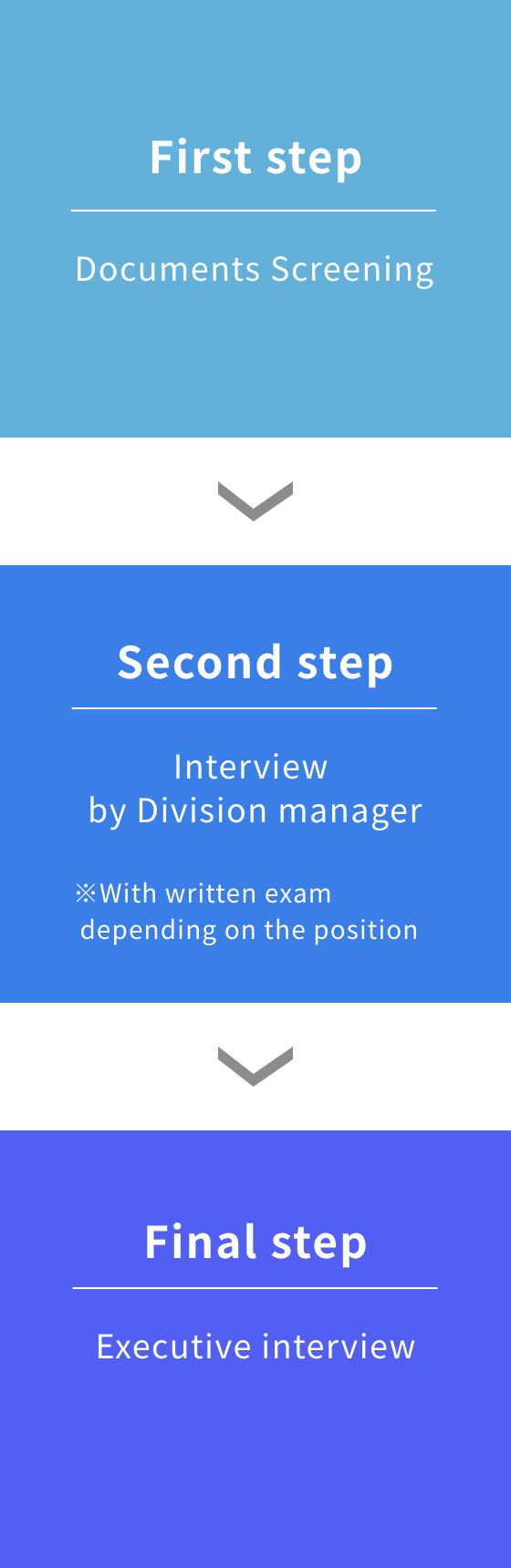
Application Process
Please note that the application process is subject to change.
First step
Documents Screening
Second step
Interview by Division manager
※With written exam depending on the positionFinal step
Executive interview