OUR SERVICE
Introduction
“SEMICONDUCTOR” is…
Indispensable for our daily life
Semiconductors, that are indispensable for our life and widely used for the familiar products such as smartphones and social infrastructure such as railways,internet and communications, take a key role in supporting our daily life. A semiconductor is a material which has intermediate properties between conductor and insulator electrically, and a main function of which is to control electric current. For example, a rice cooker can cook rice well with precise temperature control by semiconductors. Multiple semiconductors combined and integrated into a single package realize various functions and then current semiconductor products become advanced and enable us to live better and easier.
Semiconductor Manufacturing Process
Front-end Process
Design
Circuit design
Necessary functions are determined and those combination are designed with simulation based on which test specifications are determined.
Pattern design
A layout of semiconductor elements and patterns of circuit and wiring are designed.

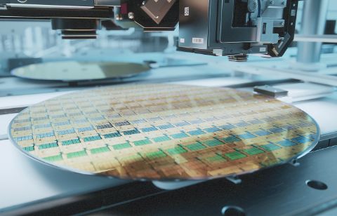
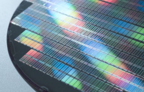
Wafer Fabrication
Deposition
Insulator and conductor films, and semiconductor films are applied onto wafers giving wafers electrical characteristics.
Photolithography
Patterns on the photomask are optically transferred onto wafers by application of a photoresist (a light-sensitive substance) to deposited wafers.
Etching
A pattern of the material on the wafers is created subject to the circuit pattern by selectively removing the deposited material film.
Cleaning/Planarization
Remaining photoresists and particles (dust) are removed, and a surface of the wafers is polished flat to form the next wiring layer after each process.
Create circuits by repeating
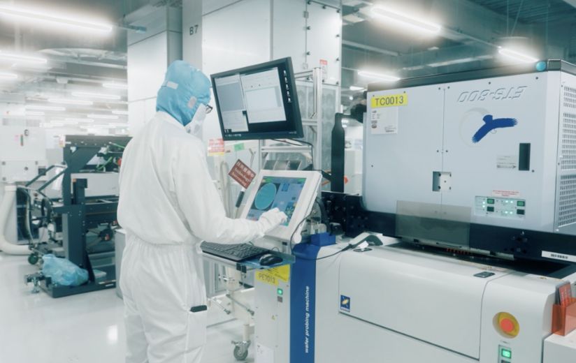
Wafer Test※
Wafer level burn-in
Potential early life failures are removed in advance through high temperature/bias reliability stress test, which may be included in a wafer test process.
Wafer test
Semiconductor wafers are verified against designed functionality with an electrical signal to check whether good or bad die. Wafer test is performed under the conditions such as low or high temperature. Those results are forwarded to the assembly process as those measurement data for assembly of only non-defective products.
Feedback of Inspection data
Failure analysis is performed with feedback of the results of wafer test.
Back-end Process
Assembly
Dicing
Each circuits formed on a wafer are cut into individual chips.
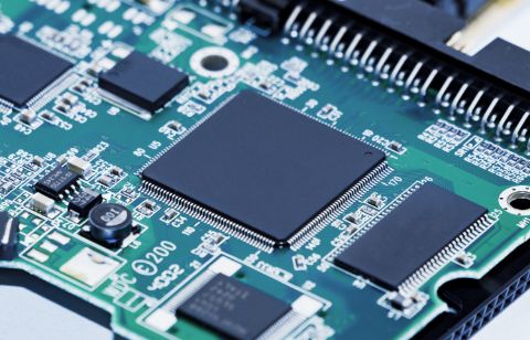
Packaging
Individual chips diced and verified as non-defective through wafer test process are sealed with ceramics and molding resin to avoid damage and corrosion, and then packaged.
Final Test※
Package burn-in
Potential early life failures are removed in advance through high temperature/bias reliability stress test when the semiconductor products require high reliability.
Final test
Each semiconductor products are verified against designed functionality with an electric signal in order to sort out to sort out those into the defective and non-defective one under the conditions such as low or high temperature.
Visual inspection/shipping packing
Packaged semiconductors are visually inspected and packed in the shipping state (tray, T&R).
Tera Probe mainly offer services for the test process (*see above diagram), and can also offer those throughout the backend processes in cooperation with our group companies.
Importance of testing

Testing for semiconductor
The electrical appliances we obtain are safe and secure. It requires strict evaluations and provision of non-defective products. A wafer test process makes it possible to evaluate the whole process up to it for the first time. The first step to provide safe products is to identify defective and non-defective products and to satisfy product specifications in the wafer test process. Feedback of those test results to the wafer manufacturing process and failure analysis contribute to raising the non-defective product rate. In addition, the wafer test process has the function to detect defects that could occur in the wafer manufacturing process when the mass production begins. This means we are responsible for provision and maintenance of high-quality products as well as management of customer’s manufacturing risks. Now that there are a type of semiconductor products combining multiple semiconductor chips into a single package where even one defective chip may make other semiconductor chips defective even if those other chips had no defect. Under this circumstances, the importance of the test process has been increasing.
We are responsible for creating a prosperous future by granting the ensured reliability to semiconductor products.
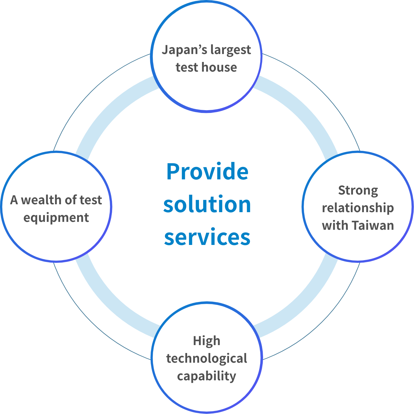
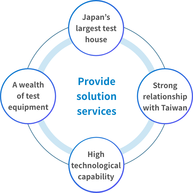
Our Strengths
-
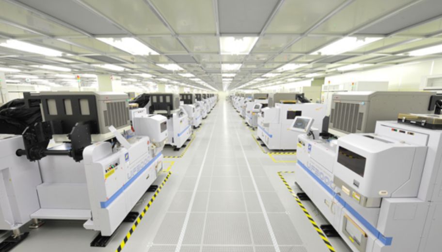
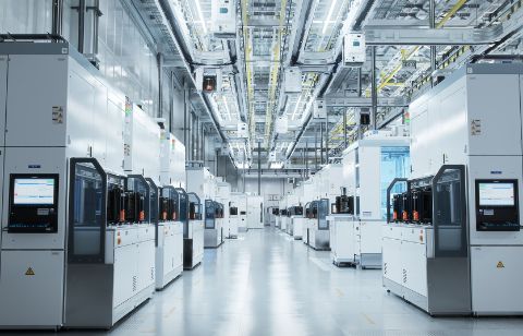
Japan’s largest test house
Tera Probe will respond to the needs in the fast-moving semiconductor industry with a state-of-the-art tester* lineup as one of the biggest test houses in Japan. * Tester: A device for inspecting the electrical characteristics of semiconductors
-
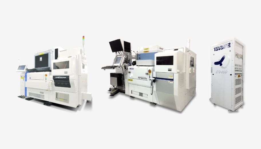
A wealth of test equipment
We have many test equipment that can cover a wide range of product applications such as logic, image sensor, analog, and memory. We are the top-class test house in Japan who can handle many different varieties of those products widely.
-
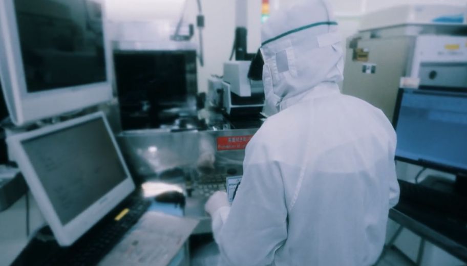
High technological capability
We have a wealth of experience and technology, as well as a lot of accumulated data, one of the best in Japan. We will offer statistical failure analysis, and propose certain improvement measures.
-

Strong relationship with Taiwan
Taiwan is the most production base of semiconductor products all over the world. We have built a close relationship with Powertech Technology Inc. (“PTI”), one of the world’s leading OSAT* companies, as our parent company located in Taiwan, and TeraPower Technology Inc., as our subsidiary. We can also offer turnkey services for the assembly process after the wafer test process through the collaboration with PTI who mainly offer services for backend manufacturing process of semiconductors. *Outsourced Semiconductor Assembly and Test (Semiconductor assembly and testing contract services)
Our Services
-
Test Operation Service
-
Test Development Service